Subtotal $0.00
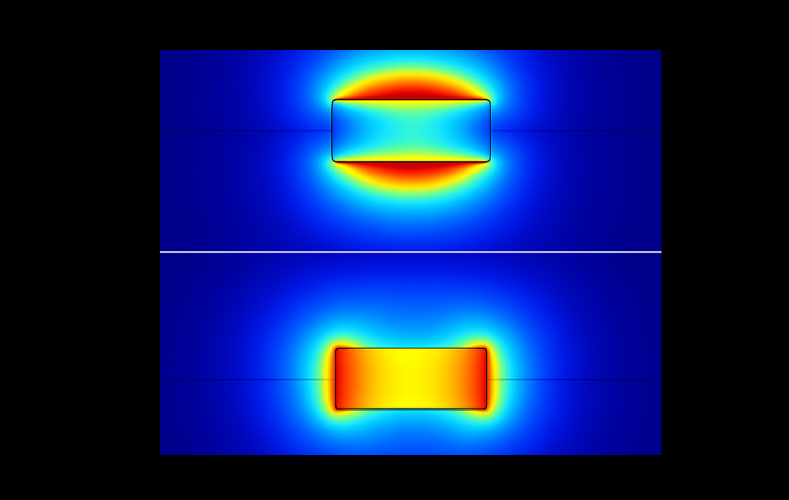

Superconducting nanowire single-photon detectors (SNSPDs) are renowned for their exceptional sensitivity, fast timing, and low dark counts, yet their performance in the mid-infrared (Mid-IR) range suffers from limited optical absorption in ultra-thin superconducting films. At longer Mid-IR wavelengths (3–12 μm), the interaction between light and nanoscale detector elements is inherently weak, reducing photon absorption and consequently lowering detection efficiency. This limitation poses a significant challenge for applications where high-efficiency Mid-IR single-photon detection is essential. The Mid-IR regime is of growing importance for technologies such as quantum communication in free space, single-photon-level thermal imaging, molecular spectroscopy, and astronomical observations. In these areas, SNSPDs could outperform other detection technologies if their absorption efficiency were improved. Achieving efficient photon coupling at these wavelengths requires innovative optical confinement schemes that can strongly localize and enhance optical fields within the active superconducting region. This project aims to design and analyze novel light-confinement strategies in ultra-thin superconducting films operating in the Mid-IR using finite-difference time-domain (FDTD) simulations. The outcome will be validated designs and guidelines that enable next-generation SNSPDs to operate with high efficiency in the Mid-IR, opening new frontiers in quantum sensing, precision spectroscopy, and infrared astronomy.
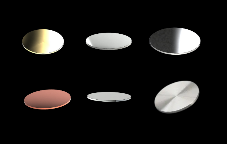
This project focuses on the simulation-driven design and optimization of new sputter targets, essential components in thin film deposition via sputtering processes. Sputter targets serve as the source material evaporated to deposit uniform thin films critical to semiconductor, optical coating, and energy device industries. However, conventional sputter target designs face challenges including non-uniform erosion, thermal stresses, and limited lifetime, leading to degradation in film quality and increased production costs. An improved understanding of sputter target behavior through simulation can guide innovative design solutions to enhance performance and durability. The two most commonly used simulation tools for this purpose are finite element method (FEM) software and Monte Carlo/molecular dynamics (MC/MD) simulations. FEM tools such as COMSOL Multiphysics and ANSYS model thermal, mechanical, and stress-related phenomena to predict temperature gradients, warping, and mechanical stresses. These insights help optimize cooling designs and material selection. MC/MD simulations, including SRIM, model plasma-target interactions, ion bombardment, and erosion at the atomic scale to predict sputtering yields and sputtered particle distributions, enabling the optimization of target geometry for uniform erosion. This project will integrate state-of-the-art FEM and MC/MD simulation tools to design sputter targets with enhanced durability, uniform erosion, and controlled thermal behavior. The goal is to develop optimized target architectures that reduce downtime, improve film quality, and extend operational lifetime in industrial sputtering applications.
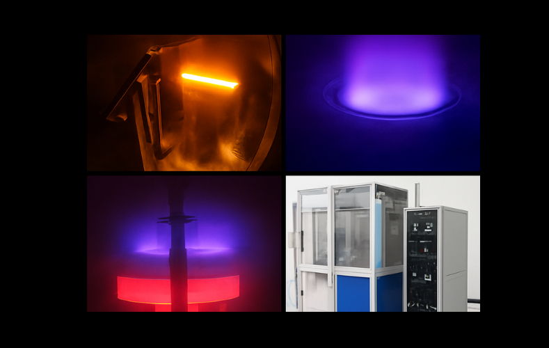
High-vacuum deposition systems, employed in semiconductor, optics, and advanced materials manufacturing, require precise environmental control to achieve uniform thin films with nanoscale accuracy. However, India and several other emerging markets largely depend on imports from developed countries due to the high capital cost, complex engineering, and stringent quality control associated with these systems. This reliance also creates barriers for startups and smaller manufacturers who face extended lead times and limited access to after-sales support. The project will analyze market data and industrial trends to identify specific gaps such as lack of indigenous technology for ultra-high vacuum chambers, precision gas handling, and automated process controls. It will evaluate how import dependence affects costs, innovation cycles, and scalability of coating technologies. Furthermore, it will explore the economic and technological feasibility of developing domestic manufacturing infrastructure and propose strategic collaborations for technology transfer and capacity building.
Conventional focal plane imaging systems rely on bulky, multi-element lenses that add complexity, aberrations, and limit device miniaturization. For next-generation compact optical and quantum photonic systems, flat and efficient focusing elements are needed. Metalenses—ultra-thin, nanostructured optical surfaces—offer precise wavefront control using subwavelength features, providing high-resolution focusing in a much smaller footprint than traditional optics. In single-photon imaging and detection, particularly with superconducting nanowire single-photon detectors (SNSPDs), efficient photon delivery to the nanoscale active region is crucial. Conventional lenses cannot focus light tightly enough to match the detector’s dimensions, reducing coupling and detection efficiency. Integrating a custom-designed metalens directly onto the detector chip enables strong field confinement and efficient photon absorption, enhancing detection rates and spatial resolution. Such integration also paves the way for scalable, high-performance imaging platforms useful in quantum communication, low-light sensing, and mid-infrared single-photon imaging. Finite-difference time-domain (FDTD) simulations will be used to design and optimize the metalens. The simulation work will include creating metasurface unit cells that achieve the desired phase profile for diffraction-limited focusing, evaluating focusing efficiency and spectral response, and optimizing geometric parameters and materials for fabrication compatibility. Near-field analyses will assess energy concentration and photon coupling efficiency at the focal plane. This project aims to develop FDTD-optimized metalens designs that achieve strong field enhancement, minimal aberrations, and high numerical aperture, enabling compact and efficient focal plane systems for single-photon detection.